FPGADesign
Custom FPGA solutions for applications where software can't keep up.
FPGA clients we've worked with


Need FPGA design
expertise?
Delivered by New Zealand's leading electronic product design team.
I need FPGA designWhat we build
From DSP algorithms to complete FPGA systems. Custom digital logic for demanding applications.
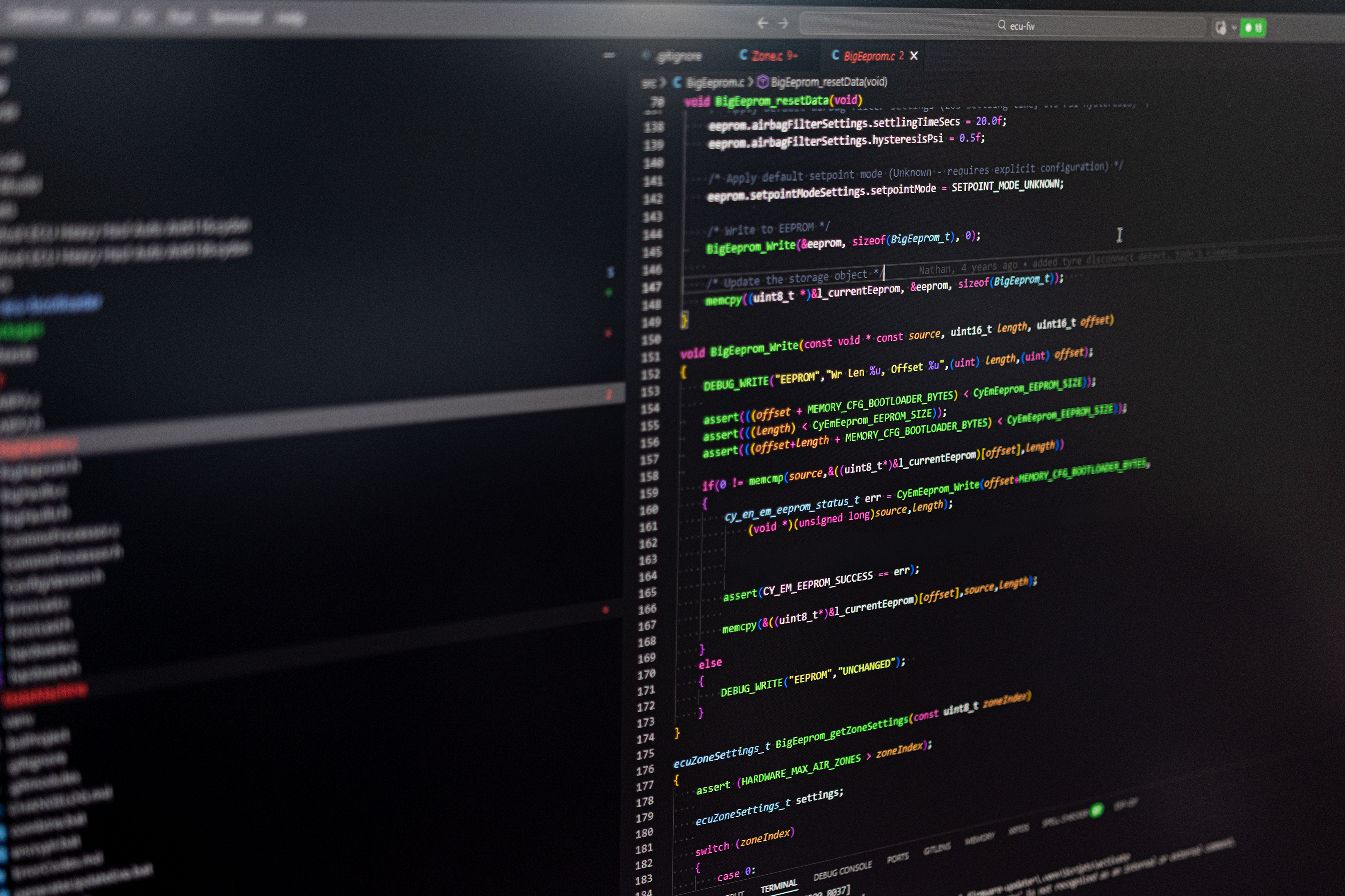
VHDL Development
Clean, synthesizable VHDL for complex digital systems. Modular architecture, testbenches, and simulation-validated designs.
Verilog Development
SystemVerilog and Verilog for high-performance designs. Timing-critical implementations with predictable behavior.
DSP Algorithm Implementation
FFT, FIR/IIR filters, correlation, and custom algorithms in hardware. Fixed-point optimization for FPGA resources.
High-Speed Data Acquisition
ADC/DAC interfaces running at hundreds of MHz. JESD204B, LVDS, and custom high-speed interfaces.
Real-Time Processing
Deterministic, microsecond-latency processing. Pipeline architectures for continuous data streams.
Image Processing
Real-time image and video processing pipelines. Camera interfaces, scaling, filtering, and feature detection.
Custom IP Core Development
Reusable IP blocks for your specific application. Well-documented, verified, and integration-ready.
FPGA-to-CPU Interfaces
AXI, PCIe, and custom interfaces to ARM processors and x86 systems. Hardware/software co-design.
Hardware Acceleration
Offload compute-intensive tasks from CPUs to FPGA fabric. Custom accelerators for machine learning, encryption, and more.
FPGA design questions
Common questions about cost, timelines, tool chains, vendor selection, and deliverables for custom FPGA and signal processing projects.
How much does an FPGA project cost?
FPGA project costs depend on the FPGA family, clocking and IO complexity, the algorithm or signal-processing pipeline, verification and timing-closure effort, and whether HDL IP, board hardware, or both are in scope. A focused engagement (HDL development on a known platform with contained scope) lands in the five-figure range. Many FPGA projects require a six-figure investment. That's especially true for designs with high-speed transceivers, complex algorithms, formal verification, or full board-and-HDL integration. Walk us through your target FPGA and what you're implementing. We'll come back with a realistic scope and budget. Get in touch.
How long does FPGA development take?
FPGA timelines depend on the complexity of the design, the performance targets, and the depth of verification required. A focused block (a custom SPI bridge, a small filter chain, a protocol converter) can be delivered in 1 to 3 months. A medium-complexity design with DSP, multiple clock domains, and standard verification runs 4 to 8 months. Full signal-processing systems with high-speed ADC/DAC interfaces, complex algorithms, formal verification, or board-and-HDL integration can extend to 12 months or more. Share what you're building and we'll come back with a realistic schedule.
When should I use an FPGA instead of a microcontroller or DSP?
Use an FPGA when firmware on an MCU or DSP can't keep up. FPGAs shine for deterministic, nanosecond-latency processing, parallel computation across many channels, custom high-speed interfaces (JESD204B, LVDS, SerDes above 1 Gbps), and algorithms like FFTs, FIR filters, or correlators running at tens to hundreds of MSPS (up to GSPS depending on the FPGA resources). If a modern ARM Cortex-M or a dedicated DSP chip can hit your throughput and latency targets, that's cheaper and faster to develop. We help clients pick the right architecture before writing a line of RTL.
Which FPGA vendors, families, and languages do you work with?
We work across all major vendors. AMD/Xilinx (Artix, Spartan, Zynq SoC, Kintex, Versal, including Series 7 and UltraScale+ architectures). We can also work with Intel Altera (Cyclone, Arria, MAX 10), Lattice (iCE40, ECP5, CrossLink), and Microchip (PolarFire, SmartFusion). Our team writes Verilog, VHDL, and SystemVerilog, and uses high-level synthesis (HLS) tools when it suits the project. Toolchains include Vivado, Vitis, Quartus Prime, Libero SoC, and Lattice Radiant/Diamond. Vendor and family selection is driven by performance, power, cost, and long-term availability for your application.
What do I receive at the end of an FPGA project?
You receive a full production package. This includes VHDL/Verilog/SystemVerilog source code, testbenches and simulation scripts, timing and pin constraint files, synthesis and place-and-route reports, the final bitstream or programming file, architecture documentation, and a user guide for any register interfaces. The exact list is agreed up front. New IP created during the engagement transfers to you on payment under our standard terms. Each party keeps their pre-existing IP. Licensing arrangements can be put in place when needed. Third-party IP licensing is flagged up front so there are no surprises.
“Beta Solutions was able to use their knowledge and skills to engineer the sensors to the demanding specifications and create a really great product. We are really happy with our experiences with Beta Solutions.”Aaron FultonRadarIQ
Want us to handle the whole product?
FPGA design is just one piece. If you don't want the headache of managing hardware, firmware, mechanical, and manufacturing separately, we handle the entire product development under one roof.
Other ways we can help
FPGA development is just one part of what we do. Explore our other services.
PCB Design
High-speed digital, RF, power electronics, and mixed-signal. Custom boards from schematic to production-ready files.
Firmware/Software Design
Bare-metal and RTOS firmware. We write the code that runs on the boards we design.
Mechanical Design
Enclosures, mounts, and housings designed around the electronics, not retrofitted after.
Volume Manufacturing
From 100 to 100,000 units. We handle the factory, logistics, and QA so you don't have to.