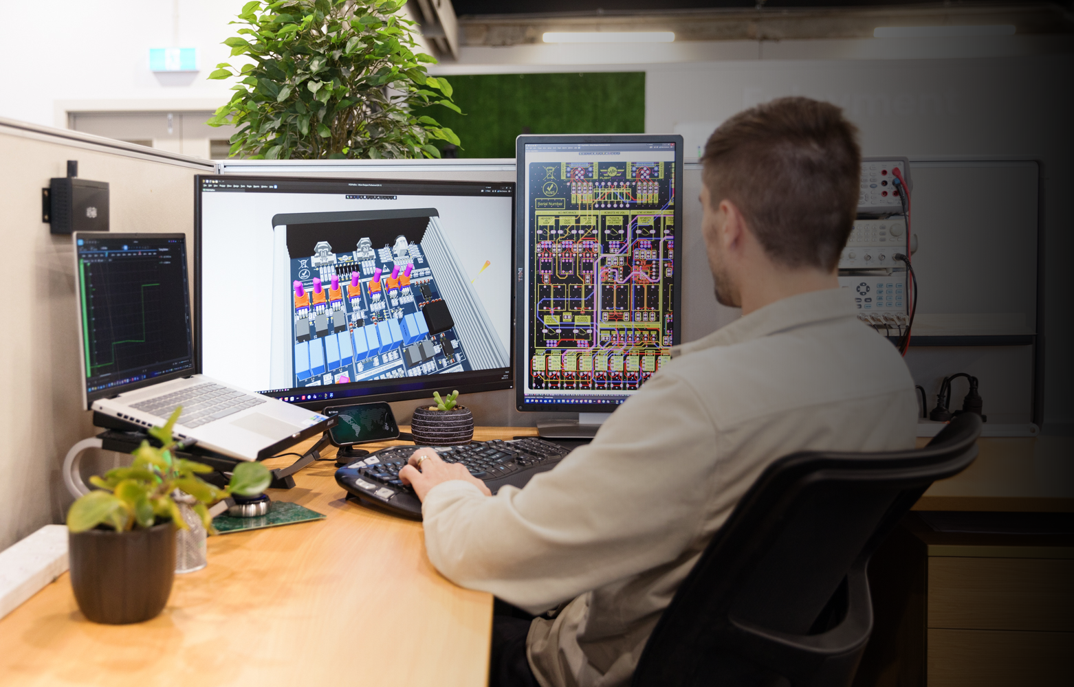
CustomPCB Design
In-house NZ electronic hardware design team who've done this hundreds of times.
Some of our clients


PCB projects we've delivered
Boards we've taken from concept to production across aviation, IoT, consumer electronics, AgTech, and more.
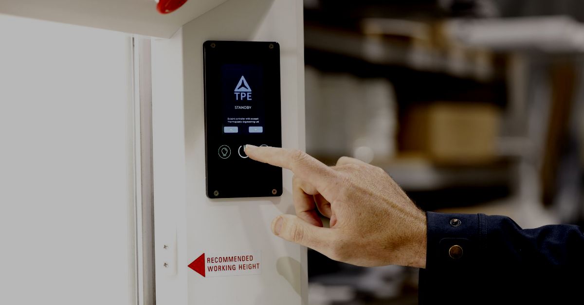
Touch Screen LCD Controller
Unified controller and touch screen display for TPE's fume cupboards. Multiple controllers consolidated into one PCB.
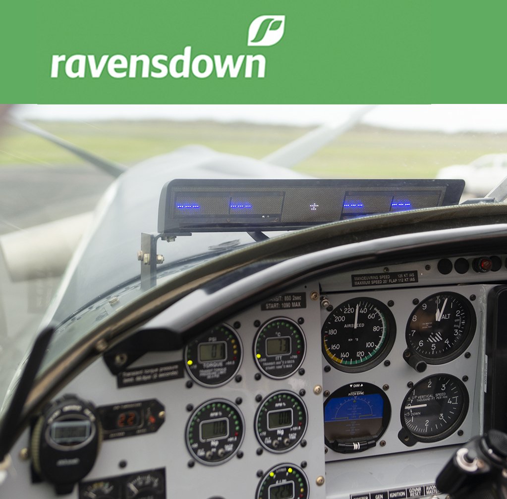
Aircraft Lightbar
Custom avionics lightbar for Ravensdown's pilots. RGB LEDs and LCD arrays built to withstand sunlight, 120-knot winds, and rain.
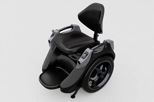
Self Balancing Personal Transport
Electronics and firmware for Omeo's award-winning self-balancing mobility vehicle, now selling globally.
Need a custom PCB
designed?
Delivered by New Zealand's leading electronic product design team.
I need a custom PCBWhat we design
Every board is different. Here's the breadth of what we handle, often all in the same design.
Microcontroller Design
ARM Cortex, STM32, ESP32, Nordic nRF. We select the right MCU for your application and design the complete system around it.
Wireless & RF
Bluetooth, WiFi, LoRa, cellular, 5G, and custom RF. Antenna matching, RF front-ends, and the layout expertise that makes wireless reliable.
Low Power Design
Battery-powered products that last. Power budgeting, sleep mode architecture, energy harvesting, and multi-year battery life targets.
Sensor Integration
Temperature, pressure, GPS, accelerometers, lidar, flow sensors. Complete signal conditioning and interface design.
FPGA & Signal Processing
Xilinx FPGA and CPLD design. VHDL, Verilog, and high-performance parallel processing for complex real-time systems.
High-Speed Digital
DDR4/5, USB 3.0+, PCIe, and GHz-class interfaces. Controlled impedance, length matching, and signal integrity simulation.
Low-Noise & Precision
Precision analog, low-noise layout, proper grounding and isolation. For measurement, scientific, and medical applications.
Power Electronics
SMPS, battery management, motor drives, and EV systems. Thermal analysis and EMC control built in from the start.
DFM & EMC
Designed for manufacturing and compliance from day one. No ambiguous BOMs, no clearance violations, no surprises.
PCB design questions
Common questions about cost, timelines, tools, and deliverables for custom PCB design projects.
How much does a PCB design project cost?
The cost of a custom PCB design varies with the complexity of the circuitry and the scope of the work. Simple boards with a low layer count start in the low thousands. Most custom projects sit in the five-figure range. Complex projects can run into six figures. This includes designs with high component counts, full regulatory certification, or production-ready handoff. Every project is different. We can usually give you a rough estimate after a quick conversation. Get in touch to discuss your project.
How long does custom PCB design take from schematic to production-ready files?
PCB design timelines depend on our availability and the complexity of the board. The main drivers are board size, layer count, RF or high-speed content, and how many design iterations are needed. Simple boards can be turned around in a few weeks. More involved projects take longer. Complex multi-layer designs with high-speed or RF content, or compliance preparation, take longest. Reach out and we'll talk through where you are and what you're trying to achieve. We can also take a project all the way from concept to production if you need it.
What PCB design software do you use?
We design primarily in Altium Designer, the industry standard for professional multi-layer PCB design. Native source files are handed over at the end of the project. You can edit, manufacture, or maintain the design with any partner, now or years from now.
Can you design multilayer, high-speed, or RF PCBs?
Yes. We design 2 to 16+ layer PCBs, including HDI, flex, and rigid-flex constructions. Our team has delivered high-speed designs with DDR4/5, USB 3.2, PCIe, and GHz-class interfaces. We also design RF boards covering Bluetooth, WiFi, LoRa, cellular (4G/LTE, NB-IoT), and custom RF front-ends. Controlled impedance, length matching, antenna matching, and signal integrity simulation are standard parts of our process.
What files and deliverables do I receive when the PCB design is complete?
You receive a full production-ready manufacturing package. This includes native source files (Altium or equivalent), schematic PDFs, Gerbers, ODB++, NC drill files, pick-and-place data, a Bill of Materials (BOM), assembly drawings, 3D STEP models, fabrication notes, and a design review document. The exact list is agreed up front. New IP created during the project transfers to you on payment. Each party keeps their pre-existing IP. We can set up licensing arrangements when needed. Of course, if we're managing production for you, we handle all of this as well. You'll also receive the finished product.
“It is rare to find the combination of high-technology technical expertise, practical hands-on skills with sophisticated and friendly customer service... Beta Solutions have such a comprehensive team to focus on each project.”Bruce RapleyAtkinson & Rapley Consulting
Want us to handle the whole product?
PCB design is just one piece. If you don't want the headache of managing hardware, firmware, mechanical, and manufacturing separately, we handle the entire product development under one roof.
Other ways we can help
PCB design is just one part of what we do. Explore our other services.
Firmware/Software Design
Bare-metal and RTOS firmware. We write the code that runs on the boards we design.
Mechanical Design
Enclosures, mounts, and housings designed around the electronics, not retrofitted after.
Volume Manufacturing
From 100 to 100,000 units. We handle the factory, logistics, and QA so you don't have to.
Design Review & Advice
We review your design and recommend changes. Expect a tighter BOM, lower unit costs, and fewer production surprises.